Design a Nand Gate Using Tools Software
Introduction
Typically when students are learning digital logic fundamentals they are limited to theoretical understanding. Multisim allows students to put this theory into practice through schematic simulation and deployment to hardware. Multisim enables you to program your Digilent teaching boards directly from the Multisim environment, making the connection between theoretical concepts and hardware implementation more understandable.
This tutorial demonstrates the process a student can go through to learn Boolean logic and illustrates how, through using Multisim, students can apply this theory to hardware to see the physical response.
Digital Logic Theory
When learning digital logic students will start with the three fundamental building blocks: AND, OR and NOT gates.
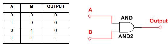
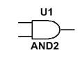
AND
Boolean Expression: AB
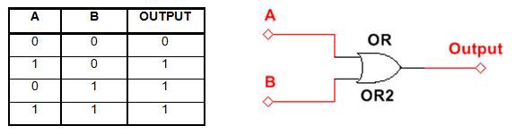
OR
Boolean Expression: A'B+AB'+AB
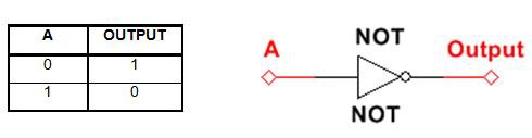
NOT
Boolean Expression: A'
Multisim allows students to interactively learn the action of these fundamental logic gates that make up the building blocks of all digital systems.
Simulation of Digital Logic
In this tutorial we will learn the action of AND gates through simulation. Multisim provides interactive components and virtual instruments to help increase students' understanding.
- Open a new blank schematic in Multisim.
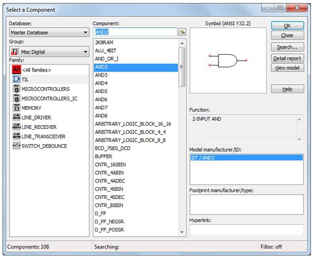
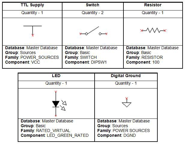
- Place down a two input AND gate from the component database. Right click and selectPlace Component.Choose the following parameters:
Database: Master Database
Group: Misc Digital
Family: TIL
Component: AND2
- Place the component on the schematic.
`
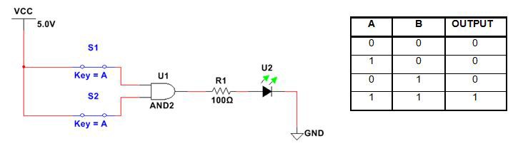
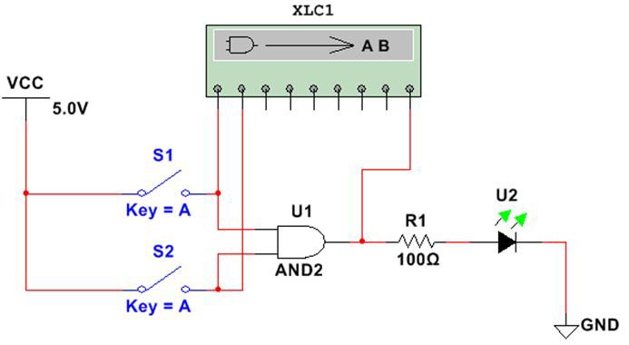
- In order to evaluate the behaviour of the component we will use a virtual switch and LED. Place the following components on the schematic.
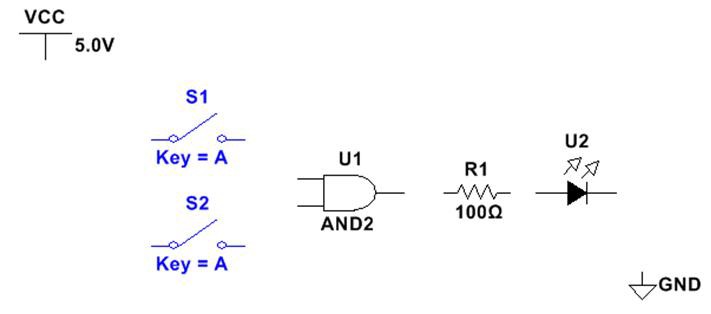
- Arrange the components on the schematic as below:
- Wire the components together to create the digital logic circuit
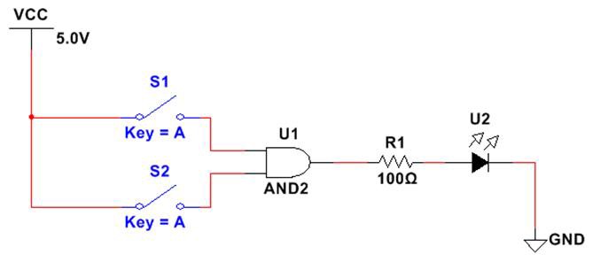
- Once we have completed our schematic we can evaluate the operation of the AND gate. The two switches and the LED are interactive components. ClickRun on the tool bar shown below.
- During execution toggle the switches and view the effect on the LED. The AND gate should respond according to the truth table below. When both switches are closed (high), the LED turns on. This allows the student to experiment with the switches to understand the AND gate operation.
- Multisim also includes interactive instruments that we can connect to our schematic, as we would benchtop instruments. In understanding digital logic theLogic Converteris a powerful tool. The Logic converter allows us to obtain a truth table and Boolean expression for our circuit. Place aLogic Converteronto the schematic.
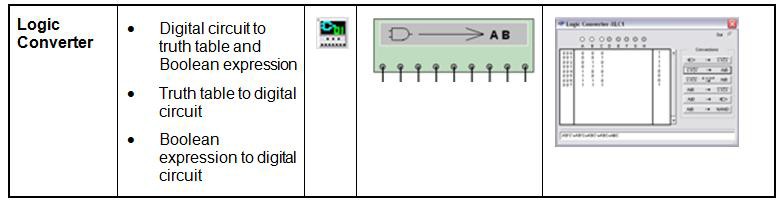
- Connect the Logic Converter to the schematic as shown below. The Logic Converter allows multiple inputs with and a single output.
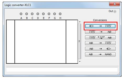
- Double click the Logic Converter to open its user interface.
- Click on the top conversion button as shown below. This is will analyze the schematic and create a truth table for the response.
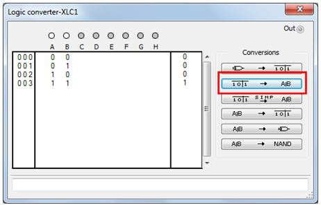
- Click on the next conversion button. This analyses the truth table and generates the Boolean expression. For an AND gate, the Boolean expression should be AB. The logic converter also allows students to input truth tables and Boolean expressions and generate logic diagrams.
- This process can be modified to allow students to gain a comprehensive knowledge of different logic gates.
Deployment of Digital Logic
Once students have gained insight through simulation of digital logic, they can continue this learning through deploying to Digilent Educational hardware.
This tutorial will provide an example of how students can create a Programmable Logic Design (PLD) and deploy this to Digilent hardware. The tutorial has been written using the Digilent Nexys 3 Board, but is the same process for all Digilent cards.
The Getting Started with Digilent Boards in Multisim tutorial will talk through the process for creating a PLD schematic for the Digilent board you are using.
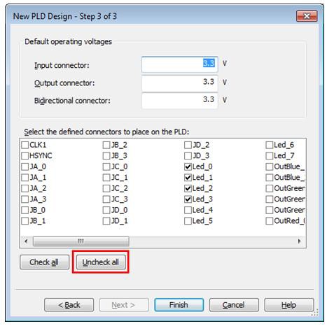
- Create a new PLD schematic for your Digilent board. Details of this process can be found within the Getting Started with Digilent Boards in Multisim. During the creation choose toUncheck allwhen selecting the IO terminals to include on the schematic.
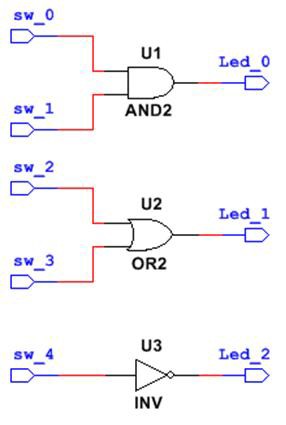
- In this tutorial we are going to create an example that allows students to gain an understanding of the functionality of OR, AND and NOT logic gates. To add IO to the schematic, select either the input or output connector from the PLD toolbar. Click theinput connector button.
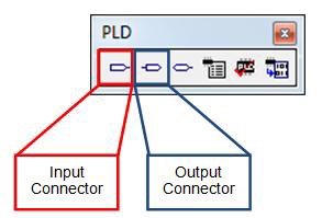
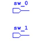
- This will display the input connector dialog and provide a list of all the IO on the Digilent board that has been designated as an input. From the list selectswitch 0 (sw_0)and clickOK.Place the terminal on the schematic.
- Repeat the process to add an input forswitch 1 (sw_1).
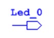
- Using the output connector button, create an output terminal for LED 0 (LED_0).
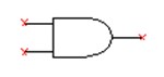
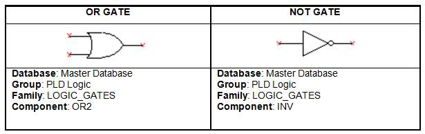
- Open the Component Database (Right click > Place component), and place a 2 input AND gate.
Database: Master Database
Group: PLD Logic
Family: LOGIC_GATES
Component: AND2
- Repeat this process to add inputs, outputs, and logic gates to demonstrate the OR and NOT gates. This will create a schematic similar to the image below.
- Once the schematic has been created, we are ready to deploy the logic schematic to the Digilent board so students can physically manipulate the switches and view the response on the LEDs. Full details on deploying to Digilent cards can be found in the Getting Started with Digilent Boards in Multisim. Select:Transfer » Export to PLD from the menu bar. Here you will see the three export options. We want to export to physical hardware so selectProgram the Connected PLD. Click Next.
- Choose theXilinx tool to compile the Multisim PLD design to a programming file. If you installed the Xilinx ISE Tools to the default location, they should autopopulate. If not, click theXilinx tool drop-down menu, selectManually select tool, and then browse to the file folder where the tools were installed. The Xilinx user constraint file contains directions that map the connectors in Multisim to the pins of the Xilinx FPGA, Part NumberXC6SLX16.
- At this point, you must connect the Digilent board to your computer. To check if all requirements have been met and the device is properly connected to Multisim, click theRefreshbutton. If the board is detected, theDevice status displays Detected -Date and Time,as shown below.
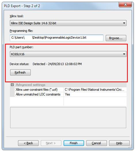
- To proceed, clickFinish. This begins the 11-step process of programming the PLD. Multisim automatically invokes the Xilinx ISE Tools (Creates the Xilinx project, Checks syntax, Translates, Places & Routes, Generates the programming file, and so on).
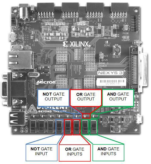
- Once the code had been generated and deployed to the Digilent board, the student can switch the switches and view the response on the integrated LEDs.
Design a Nand Gate Using Tools Software
Source: https://knowledge.ni.com/KnowledgeArticleDetails?id=kA03q000001DpNLCA0
0 Response to "Design a Nand Gate Using Tools Software"
Post a Comment